http://arstechnica.com/

Intel
ISSCC 2015, being held in San Francisco this week, is where all the big players in silicon (Intel, Samsung, TSMC, IBM, etc.) meet to talk about their latest manufacturing processes and how they might go about overcoming the current barriers to smaller, faster, and denser computer chips. It's not unusual for Intel to have one of the largest presences at the conference, and this year is no different: it will be presenting three papers on its 14nm technology, hosting sessions on a variety of topics, and Mark Bohr—one of Intel's most esteemed researchers—will be sitting on a panel that discusses Moore's law beyond 10nm.

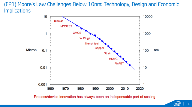
The steady march of new CMOS processes driving ever smaller transistors.
Intel
More interesting than 10nm, though, is the news that Intel is looking to move away from silicon FinFETs for its 7nm process. While Intel didn't provide any specifics, we strongly suspect that we're looking at the arrival of transistors based on III-V semiconductors. III-V semiconductors have higher electron mobility than silicon, which means that they can be fashioned into smaller and faster (as in higher switching speed) transistors. The topic of extreme UV (EUV) lithography also came up during the call, but due to continued problems with EUV deployment, it sounds like Intel is planning to do both 10nm and 7nm without it.

Intel
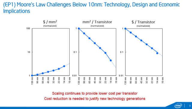
With 10nm, Intel hopes to carry the mantle of Moore's law forward to yet another node while continuing to decrease the price per transistor—in other words, we'll continue to see chips that consume slightly less power while also integrating yet more features onto a single die. 7nm, with a possible shift away from silicon, is more exciting; transistors fashioned out of III-V semiconductors can consume much less power while switching at much higher speeds. Individually, neither of these new processes are likely to raise the roof; but a 3D stack of 7nm dies... now we're talking.
No comments:
Post a Comment