http://arstechnica.com/
As tough as graphene, with electronic properties that differ based on orientation.

The structure of a borophene cluster.
Now, an unusual atom—boron—has been used to produce a novel 2D material called "borophene."
Boron at the atomic level
Boron is one of the many materials that has been considered for development of 2D materials. Boron is an interesting atom to use as a building block for a number of reasons. First, it is a semi-metal, meaning it exhibits some properties of metals and some properties of nonmetals; as a 2D material, it thus has the potential to exhibit unique behavior.Additionally, boron has interesting bonding capabilities. It has three valence electrons in the p-orbital, meaning that it can form up to three bonds. Boron can form strong covalent bonds, with two electrons split between two atoms, or stable electron-deficient bonds, with two electrons split between three atoms. As a result, boron can form materials with different three-dimensional patterns.
When it comes to producing 2D boron, however, the majority of boron studies have been theoretical in nature; few experiments were done due to the costly and toxic precursors that seemed necessary. Recently, in an investigation published in Science, scientists have managed to make 2D boron without relying on these precursors. They call their atomically thin film "borophene."
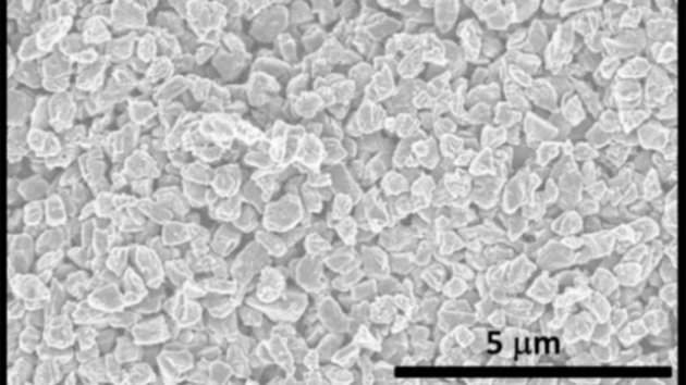
A new 2D boron sheet
In the new study, scientists grew boron sheets using physical vapor deposition. In this method, boron is evaporated in an ultra-high vacuum. Under vacuum, the evaporated particles travel toward the target surface (in this case, silver) and deposit to form a thin film. Depending on the orientation of the boron to the silver surface and on the deposition conditions, a variety of 2D boron structures will form.Characterization of the borophene films revealed that certain films displayed similarities to the model “borophene” molecule structure, which consists of 36 boron atoms forming three interconnected, quasi-planar rings around a hexagonal central hole. However, instead of forming individual molecules, the new films were composed of layers of these rings, exhibiting out-of-plane buckling. These fragments orient themselves to form a hexagonal structure with a boron atom sitting in the center, much like a bee resting in a honeycomb within a nest. Other structures were also seen, including a ribbon-like material.
Electronic characterization of the films revealed that they are metallic but that their electronic properties depend on the direction in which the current flows. In other words, electrons moved differently as they crossed the borophene in different directions (the technical term for this is "anisotropic electronic properties").
Borophene vs. other 2D materials
From a fundamental perspective, the 2D borophene layer is truly interesting. It represents the missing link between fully covalently bound 2D materials—such as graphene—and films of semi-metals that are only stable when they're layered on a specific support structure—like silicene (a non-planar, buckled layer of the semi-metal silicon).Borophene layers are more stable than silicene due to their strong covalent interactions. Additionally, borophene layers boast similar mechanical properties to graphene. In this case, the borophene layers have different mechanical properties in perpendicular directions. In comparison to graphene, which has a Young's modulus of 340 GPa-nm, borophene layers exhibit a higher Young’s modulus along one axis (398 GPa-nm) and a lower one along the perpendicular axis (170 GPa-nm). The borophene layer films also have considerable toughness.
No other 2D material has the properties of the new borophene layers, which have the capability to interface with metals, semi-metals, and nonmetals. As a result, single and multiple borophene layers offer a broad avenue for development of nano-scale electronic devices and micro-scale mechanical devices. However, future integration into commercial applications hinges on the ability to develop a fabrication method that provides more uniformity, rather than producing multiple versions of the material.
Scientists have developed a way to create diamonds without high heat or pressure

By Ed Oswald
December 2, 2015 4:17 PM
Previously there was thought to only be two solid forms of carbon: graphite and diamond. Graphite is pretty common, although diamonds are found much less often. This is because it takes a substantial amount of pressure and heat to produce a diamond, and the type of conditions for this to happen on Earth haven’t existed for more than a billion years.
Even in the lab, synthetic diamond-makers still must recreate these conditions to get the process to work. That’s a big expense, so the fact that NC State researchers are able to do this without any atmospheric modifications is pretty incredible.
Related: Can you make diamonds faster and cheaper? A Silicon Valley startup says yes
“We can create diamond nanoneedles or microneedles, nanodots, or large-area diamond films, with applications for drug delivery, industrial processes and for creating high-temperature switches and power electronics,” lead research and NC State professor Jay Narayan says.
Narayan noted that Q-Carbon is harder than a diamond, and will glow even when exposed to small amounts of energy. It may show promise for use in new display technologies as well he says, although a lot of research is still needed to understand its properties completely.
Other companies have worked on ways to produce synthetic diamonds on the cheap, such as Santa Clara, Calif.-based Diamond Foundry. However, that company still uses high heat and pressure to produce its gems, which isn’t much different from how diamonds are are produced naturally.
The researchers are still learning how to manipulate Q-Carbon, although in the meantime have filed two provisional patents on both Q-Carbon itself and the diamond production technique used to create it. Researchers did not say when they expect the technique to be ready for commercial use.
No comments:
Post a Comment