From Wikipedia, the free encyclopedia

Intel C4004 microprocessor
|
|
| Produced | From late 1971 to 1981 |
|---|---|
| Common manufacturer(s) |
|
| Max. CPU clock rate | 740 kHz |
| Min. feature size | 10μm |
| Instruction set | 4-bit BCD oriented |
| Application | Busicom calculator, arithmetic manipulation |
| Successor | Intel 4040 Intel 8008 |
| Package(s) |
|
Contents
History and production

Faggin, the sole chip designer among the engineers on the MCS-4 project, was the only one with experience in MOS random logic and circuit design. He also had the crucial knowledge of the new silicon gate process technology with self-aligned gates, which he had created at Fairchild in 1968. At Fairchild in 1968, Faggin also designed and manufactured the world's first commercial IC using SGT, the Fairchild 3708.[3] As soon as he joined the Intel MOS Department he created a new random logic design methodology based on silicon gate, and contributed many technology and circuit design inventions that enabled their single chip microprocessor to become a reality. His methodology set the design style for all the early Intel microprocessors and later for the Zilog Z80. He also led the MCS-4 project and was responsible for its successful outcome (1970–1971). Marcian "Ted" Hoff, head of the Application Research Department, contributed the architectural proposal for Busicom working with Stanley Mazor in 1969, then he moved on to other projects. When asked where he got the ideas for the architecture of the first microprocessor, Hoff related that Plessey, "a British tractor company", had donated a minicomputer to Stanford, and he had "played with it some" while he was there. Shima designed the Busicom calculator firmware and assisted Faggin during the first six months of the implementation. The manager of Intel's MOS Design Department was Leslie L. Vadász.[4] At the time of the MCS-4 development, Vadasz's attention was completely focused on the mainstream business of semiconductor memories and he left the leadership and the management of the MCS-4 project to Faggin.
Busicom had designed their own special purpose LSI chipset for use in their Busicom 141-PF calculator with integrated printer, following the architectural model of the Olivetti Programma 101, the world’s first tabletop programmable calculator, introduced in 1965, and commissioned Intel to develop it for production. However, Intel determined it was too complex, since serial memories required more components, and would use 40 pins, a packaging standard different from Intel’s own 16-pin standard and so it was proposed that a new design produced with standard 16-pin DIP packaging and reduced instruction set be developed.,[5] using Intel’s newly developed dynamic RAM memory. This resulted in the 4004 architecture, which was part of a family of chips, including ROM, DRAM and serial to parallel shift register chips. The 4004 was subsequently designed using silicon gate technology and built of approximately 2,300 transistors[6] and was followed the next year by the first ever 8-bit microprocessor, the 3,500 transistor 8008 (and the 4040, a revised and improved 4004). It was not until the development of the 40-pin 8080 in 1974 that the address and data buses would be separated, giving faster and simpler access to memory.
The 4004 employed a 10 µm process silicon-gate enhancement load pMOS technology and could execute approximately 92,000 instructions per second; a single instruction cycle was 10.8 microseconds.[7] The original clock speed design goal was 1 MHz, the same as the IBM 1620 Model I.[citation needed]
The Intel 4004 was designed by physically cutting sheets of Rubylith into thin strips to lay out the circuits to be printed, a process made obsolete by current computer graphic design capabilities.[8]
Name and variants

Tadashi Sasaki attributes the basic invention to break the calculator into four parts with ROM (4001), RAM (4002), shift registers (4003) and CPU (4004) to an unnamed woman from the Nara Women's College present at a brainstorming meeting that was held in Japan prior to his first meeting with Robert Noyce from Intel, leading up to the Busicom deal.[10]
The 4004 was part of the MCS-4 family of LSI chips that could be used to build digital computers with varying amounts of memory. The other members of the MCS-4 family were memories and input/output circuits, which are necessary to implement a complete computer. The 4001 was a ROM (read-only memory) with four lines of output; the 4002 was a RAM (random access memory) with four lines of input/output. The 4003 was a static shift register to be used for expanding the I/O lines, for example, for keyboard scanning or for controlling a printer.
The 4004 included control functions for memory and I/O, which are not normally handled by the microprocessor.
Technical specifications


| Intel 4004 registers | |||||||||||||||||||||||||||||||||||||||||||||||||||||||||||||||||||||||||||||||||||||||||||||||||||||||||||||||||||||||||||||||||||||||||||||||||||||||||||||||||||||||||||||||||||||||||||||||||||||||||||||||||||||||||||||||||||||||||||||||||||||||
|
|||||||||||||||||||||||||||||||||||||||||||||||||||||||||||||||||||||||||||||||||||||||||||||||||||||||||||||||||||||||||||||||||||||||||||||||||||||||||||||||||||||||||||||||||||||||||||||||||||||||||||||||||||||||||||||||||||||||||||||||||||||||
- Maximum clock speed was 740 kHz
- Instruction cycle time: 10.8 µs[11] (8 clock cycles / instruction cycle)
- Instruction execution time 1 or 2 instruction cycles (10.8 or 21.6 µs), 46300 to 92600 instructions per second
- Separate program and data storage. Contrary to Harvard architecture designs, however, which use separate buses, the 4004, with its need to keep pin count down, used a single multiplexed 4-bit bus for transferring:
- 12-bit addresses
- 8-bit instructions
- 4-bit data words
- Instruction set contained 46 instructions (of which 41 were 8 bits wide and 5 were 16 bits wide)
- Register set contained 16 registers of 4 bits each
- Internal subroutine stack 3 levels deep.
Support chips
- 4001: 256-byte ROM (256 8-bit program instructions), and one built-in 4-bit I/O port. A 4001 ROM+I/O chip cannot be used in a system along with a 4008/4009 pair.[citation needed]
- 4002: 40-byte RAM (80 4-bit data words), and one built-in 4-bit output port; the RAM portion of the chip is organized into four "registers" of 20 4-bit words:
- 4003: 10-bit parallel output shift register for scanning keyboards, displays, printers, etc.
- 4008: 8-bit address latch for access to standard memory chips, and one built-in 4-bit chip select and I/O port
- 4009: program and I/O access converter to standard memory and I/O chips
- 4269: keyboard/display interface
- 4289: memory interface (combined functions of 4008 and 4009)
Construction
Numerous versions of the Intel MCS-4 line of processors were produced. The earliest versions were ceramic and used a Zebra pattern of white and gray on the back of the chips. The next generation of the chip was plain white ceramic. Current versions of MCS-4 family are produced with plastic. Collectors of these chips have peaked in recent years due to the significance that is associated with this achievement.Use
The first commercial product to use a microprocessor was the Busicom calculator 141-PF.According to Nick Tredennick, a microprocessor designer and expert witness to the Boone/Hyatt patent case[clarification needed]:
Here are my opinions from [the] study [I conducted for the patent case]. The first microprocessor in a commercial product was the Four Phase Systems AL1. The first commercially available (sold as a component) microprocessor was the 4004 from Intel.A popular myth has it that Pioneer 10, the first spacecraft to leave the solar system, used an Intel 4004 microprocessor. According to Dr. Larry Lasher of Ames Research Center, the Pioneer team did evaluate the 4004, but decided it was too new at the time to include in any of the Pioneer projects.[citation needed] The myth was repeated by Federico Faggin himself in a lecture for the Computer History Museum in 2006.[13]
— [12]
Legacy and value
On November 15, 2006, the 35th anniversary of the 4004, Intel celebrated by releasing the chip's schematics, mask works, and user manual.[14]On October 15, 2010, Faggin, Hoff, and Mazor were awarded the National Medal of Technology and Innovation by President Barack Obama for their pioneering work on the 4004.[15]
References
- Jump up ^ http://www.cpu-world.com/CPUs/4004/index.html Intel 4004 microprocessor family, retrieved 2011 Dec 14
- Jump up ^ Gilder, George (1990). Microcosm: the quantum revolution in economics and technology. Simon and Schuster. p. 107. ISBN 978-0-671-70592-3. "Intel's first advertisement for the 4004 appeared in the November 15, 1971 issue of Electronic News,"
- Jump up ^ Earliest Published Papers, retrieved 2012 Jan 16
- Jump up ^ "The Intel4004". Intel4004.com. Retrieved 2008-03-15.
- Jump up ^ Nigel Tout. "The Busicom 141-PF calculator and the Intel 4004 microprocessor". Retrieved November 15, 2009.
- Jump up ^ "Intel 4004 Fun Facts". Intel.com. Retrieved 2011-07-06.
- Jump up ^ "Intel 4004 datasheet" (PDF). Retrieved 2011-07-06.
- Jump up ^ "Intel's Accidental Revolution". CNet.com. Archived from the original on 2012-07-11. Retrieved 2009-07-30.
- Jump up ^ "The Intel4004". Intel4004.com. Retrieved 2012-08-21.
- Jump up ^ Aspray, William (1994-05-25). "Oral-History: Tadashi Sasaki". Interview #211 for the Center for the History of Electrical Engineering. The Institute of Electrical and Electronics Engineers, Inc. Retrieved 2013-01-02.
- Jump up ^ Intel's museum archive i4004 datasheet
- Jump up ^ "Dissertation 2004" (PDF). Retrieved 2011-07-06.
- Jump up ^ "Intel 4004 Microprocessor 35th Anniversary". YouTube. Retrieved 2011-07-06.
- Jump up ^ Intel 4004 Microprocessor Historical Materials, Intel Museum, 2009-11-15, accessed 2009-11-18
- Jump up ^ "President Obama Honors Nation's Top Scientists and Innovators" (Press release). October 15, 2010.
Patents
- US 3753011 August 14, 1973. Faggin, Federico: Power supply settable bi-stable circuit.
- US 3821715 June 28, 1974. Hoff, Marcian; Mazor, Stanley; Faggin, Federico: Memory system for multi-chip digital computer.
Historical documents
- Faggin F., Capocaccia F. "A New Integrated MOS Shift Register”, Proceedings XV International Electronics Scientific Congress, Rome, April 1968, pp. 143–152. This paper describes a novel static MOS shift register, developed at SGS-Fairchild (now ST Micro) at the end of 1967, before Federico Faggin joined Fairchild's R&D in Palo Alto (Ca) in February 1968. Faggin later used this new shift register in the MCS-4 chips, including the 4004.
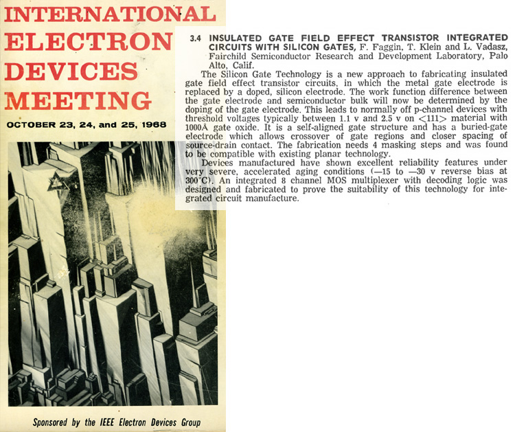
- Cover and abstract of the IEDM (International Electron Devices Meeting) Program (October 1968). The Silicon Gate Technology (SGT) was first presented by its developer, Federico Faggin, at the IEDM on October 23, 1968 in Washington, D.C. It was the only commercial process technology for the fabrication of MOS integrated circuits with self-aligned gate that was later universally adopted by the semiconductor industry. The SGT was the first technology to produce commercial dynamic RAMs, CCD image sensors, non volatile memories and the microprocessor, providing for the first time all the fundamental elements of a general purpose computer with LSI integrated circuits.
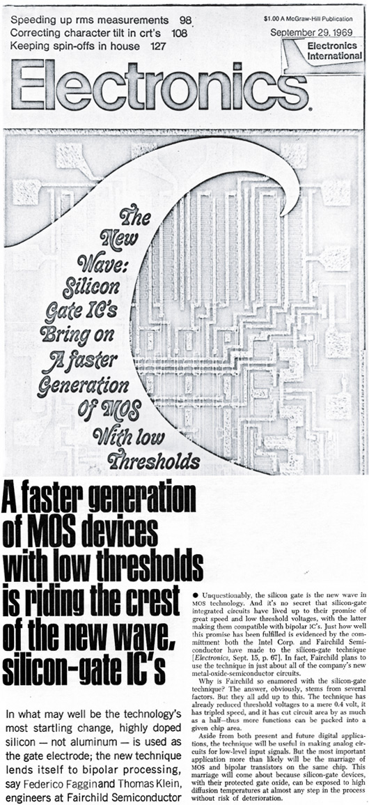
- Cover of Electronics Magazine (September 29, 1969). The Electronics article introduces the Fairchild 3708, designed by Federico Faggin in 1968. It was the world's first commercial integrated circuit using the Silicon Gate Technology, proving its viability.
- Initials F.F. (Federico Faggin) on the 4004 design (1971). The 4004 bears the initials F.F. of its designer, Federico Faggin, etched on one corner of the chip. Signing the chip was a spontaneous gesture of proud authorship and was also an original idea imitated after him by many Intel designers.
- Busicom Calculator Engineering Prototype (1971). (Gift of Federico Faggin to the Computer History Museum, Mountain View, CA). The CHM collection catalog shows pictures of the engineering prototype of the Busicom 141-PF desktop calculator. The engineering prototype used the world’s first microprocessor to have ever been produced. This one-of-a-kind prototype was a personal present by Busicom’s president Mr. Yoshio Kojima to Federico Faggin for his successful leadership of the design and development of the 4004 and three other memory and I/O chips (the MCS-4 chipset). After keeping it in his home for 25 years, Faggin donated it to the CHM in 1996.
- F. Faggin and M.E. Hoff: "Standard parts and custom design merge in four-chip processor kit". Electronics/April 24, 1972, pp. 112–116
- F. Faggin, M.Shima, M.E. Hoff, Jr., H. Feeney, S. Mazor: "The MCS-4 An LSI micro computer system". IEEE '72 Region Six Conference
Further reading
- Federico Faggin, Marcian E. Hoff Jr., Stanley Mazor and Masatoshi Shima. The history of the 4004. IEEE Micro, 16(6):10-20, December 1996. "The 4004 design team tells its story."
- Intel 4004 Microprocessor 35th Anniversary - Live recording of presentations by Ted Hoff and Federico Faggin at the Computer History Museum for the 35th anniversary of the first microprocessor. (youtube.com)
- IEEE Solid State Circuits Magazine, Winter 2009 Vol.1 No.1. "The 4004 microprocessor of Faggin, Hoff, Mazor, and Shima".
External links
- Intel's First Microprocessor—the Intel 4004: Intel Museum (Intel Corporate Archives) entry
- The Intel 4004: A testimonial from Federico Faggin, designer of the 4004 and developer of its enabling technology
- The New Methodology for Random Logic Design Used in the 4004 and in All the Early Intel Microprocessors
- Interview with Masatoshi Shima
- MCS-4 Micro Computer Set Data Sheet (12 pp)
- Intel 4004 schematics at the unofficial 4004 website, and a simulator in Java
- The Crucial Role of Silicon Design in the Invention of the Microprocessor
- High resolution light microscope pictures of an Intel 4004 die together with a basic explanation of CMOS logic
- Intel 4004 Assembler and Disassembler: Simple programming tools for Intel 4004 in Javascript
- Datasheet Intel 4004
- Datasheet Intel MCS-4
No comments:
Post a Comment