The world’s first nine dollar computer has more ports than the MacBook
http://www.digitaltrends.com/
Microcontrollers like Arduino and Raspberry Pi
have become very popular in recent years, but their functionality
is primarily aimed at hobbyists and coders, rather than being a
small-scale computer in their own right. Now, a new product on
Kickstarter looks set to make the idea of a microcomputer more
attainable than ever.
That device is the CHIP, and it comes from Next Thing Co.
It can do all the basic tasks you would expect from any other
computer; you can use it to do some word processing, check your emails,
even play video games — but this computer can be yours for just nine
dollars.
For that price, you’ll get a tiny board that you can
hook up to any monitor and keyboard and put to use. It comes
pre-installed with a host of useful open source software, including
LibreOffice, the Chromium web
browser and coding tool Scratch. The device includes built-in wireless,
Bluetooth 4.0, USB, micro-USB, and an audio jack. There’s also 4GB of
flash storage. Notably, it’s missing an SDcard reader for easy storage
expansion.
The device’s campaign page
on Kickstarter describes it as the world’s first nine dollar computer,
and if it works as it says it does, it will be a pretty impressive piece
of tech. Obviously, other hardware like a display and a keyboard costs
money too — but it’s a sure sign that we’re living in a future when you
can buy a functional computer with a ten dollar bill and get change.
For
a pledge of $49, you’ll also get a housing for the C.H.I.P. that makes
it into a portable device, complete with a 4.3″ touchscreen and
miniature QWERTY keyboard. A nifty design quirk allows you to slot a
pencil through a small hole towards its base and use it as a kickstand. Related:Microsoft releases Windows 10 IoT preview
The CHIP Kickstarter is attempting to raise $50,000 to fund the first production run of the device, and is set to run until June 6, 2015.
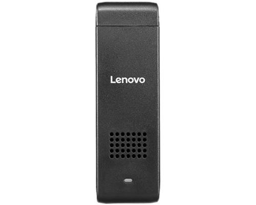
Lenovo’s new PC on a stick is a full Windows PC that can be plugged into any PC or monitor with an HDMI port. (Lenovo)
Lenovo is hitting a new PC market in a small way.
On Tuesday, the popular PC vendor announced its latest creation – a PC on a stick.
Starting at $130, the new Ideacentre Stick 300 is designed to deliver
the performance of a Windows PC but in a bite-sized portion. The mini-PC
is only 3.94 inches wide, 1.5 inches deep and .59 inches high, so it’s
not much larger than your average USB stick.
Why
a PC on a stick? Portability is the main draw. You can carry the
Ideacentre Stick 300 with you on the go and plug it into any TV or PC
monitor with an HDMI port to run its onboard applications and access
your files. Beyond that, the idea is to offer consumers a device with
enough computing power to let you play games, surf the Web and chat with
friends via video without having to purchase a pricey tablet or laptop.
This
is also a new market for Lenovo, which is already No. 1 in the
worldwide PC market and No. 3 in the smartphone market. The mini PC
represents a new challenge in which the company will compete with other
PC-on-a-stick makers, such as Intel and Microsoft.
Powered
by an Intel Atom processor, the Ideacentre Stick 300 carries up to 2
gigabytes of memory and up to 32GB of onboard storage. Wi-Fi and
Bluetooth 4.0 are also included for wireless connectivity. One HDMI
port, one MicroUSB 2.0 port and one SD card reader come along for the
ride, along with a small speaker.
The
stick comes with Windows 8.1, but will be eligible to upgrade to
Windows 10 when Microsoft releases its new operating system on July 29. A
three-month trial of Microsoft Office is also part of the package. The
only items you’ll need to add to use the stick are a wireless keyboard
and mouse.
“We’ve
looked at the computing needs of travelers, business people and
families, and realized that a truly portable and affordable solution
would be a significant benefit to users of all kinds,” Jun Ouyang,
Lenovo’s general manager for Worldwide Desktop and Visuals, said in a
press release. “Our goal with the Ideacentre Stick 300 is to give those
users a sense of freedom and enhanced mobility, while packing a serious
punch in a small device.”
Starting in July, the Ideacentre Stick 300 will be up for sale on Lenovo’s website as well as at various retail stores.
Intel Compute Stick Turns Any TV Into A Windows PC For Just $149
Intel wants to help you turn any TV into a Windows PC, for the low cost of $149. All it takes is a little stick, much like the much-loved Google Chromecast. Meet the all-new Intel Compute Stick.
The
Compute Stick is essentially a complete PC, but in the compact form
factor of a slightly large pen drive. It connects to a TV via HDMI, but
also has to be powered with a microUSB cord. Here’s a quick look at the
important specs:
1.33GHz quad-core Intel Atom Z3735F processor
2GB DDR3 RAM
32GB internal storage
MicroSD slot (up to 128GB)
Wi-Fi 802.11 b/g/n
Bluetooth 4.0
Full-size USB port
HDMI 1.4
Windows 8.1 Bing
It
will also be available with Linux, but that version will come with 8GB
of storage and 1GB RAM. That model will retail for $89, Intel said. Check out the full specs.
The Z3735F processor does not support 4K hardware decoding.
Windows 8.1 Bing looks and behaves just like Windows 8.1—it’s a
low-resource version preset to have Bing in all the search engines, but
you can manually change that.
Why The Intel Compute Stick Matters
While smart TVs are on the rise, you probably won’t use all of their features.
That’s because it’s not a full-fledged desktop operating system running
there. You can’t run Microsoft Office on your smart TV, after all.
Google’s
Chromecast streams content from other connected devices. You can’t use
the Chromecast without a second phone, tablet or computer. But the
Compute Stick will just need a Bluetooth keyboard and mouse or some fantastic wireless all-in-one keyboards to be up and running.
The current lot of Android Stick PCs are good for gaming and multimedia,
but Android itself can’t compare to Windows when it comes to getting
work done in a desktop environment. Similarly, the Roku Streaming Stick (read our review) is great for watching movies and TV shows, but little else.
Plus, at $149, it’s still far cheaper than our recommended DIY HTPC build. And yes, you can turn it into a Roku-like streaming device for free.
More Than Just A Media Player
The Intel Compute Stick is for more than just multimedia though.
Essentially, this is a complete PC you can carry around with you
anywhere you go. In fact, it’s your PC on a stick—connectable to any device with an HDMI port.
CNET got some hands-on time with the Compute Stick and describes how it would be useful:
As
someone who likes to travel but loathes toting a laptop around, keeping
something like this with a Bluetooth keyboard and mouse in my luggage
would be a compact way to get a more robust computing experience than my
iPad is going to offer, without tipping the scales or putting much of a
dent in my wallet. I don’t expect to be able to edit photos or play
World of Warcraft while I’m on the road, but this could prove to be a
great tool for toting vital files and Windows apps around, and getting
the full-PC experience wherever I can find a spare HDMI port.
Tom’s Guide echoes this opinion, stressing it will be fine for the usual multimedia requirements, but it can also do a bit more:
Atom
Baytrail processors are not great for gaming or crunching video, but
they can handle light productivity work, Web surfing, email and social
networking very smoothly.
You Can Buy One Right Now! (But It’s Not Officially From Intel)
Intel
has said it will be selling the Compute Stick directly, and that it
will launch later this year. If you’re in the market for an HTPC, you
might want to wait it out if you can.
However, if you aren’t too worried about the Intel branding, you can grab one of these right now. As Liliputing points out, Chinese company MeegoPad is already selling the exact same model.
The
MeegoPad T01/TB05 has the same hardware as the Compute Stick, complete
with an Intel logo to prove its legitimacy. You can buy it for $115 on Amazon. GizChina got its hands on the MeegoPad T01
and says it runs Windows 8.1 out of the box, and it looks like a pretty
neat device, as you can see in the unboxing video. However, on Amazon,
we weren’t able to ascertain if these devices shipped with Windows 8.1
preloaded on them or not—they all strategically say it “supports Windows
and Android”, so we’d exercise caution.
If you’re willing to
risk the $140, the MeegoPad T01 seems like a good way to get your hands
on the Intel Compute Stick early, but be warned that you might have to
load Windows yourself. Here’s how to install Windows 8 from a USB stick. Will you wait for Intel’s Compute Stick, buy the MeegoPad T01, or are you happy with something like the Roku Streaming stick? Image credits: Ambrozjo (FreeImages), CianDesign (DeviantArt), Intel (WSJ), Intel, Microsoft
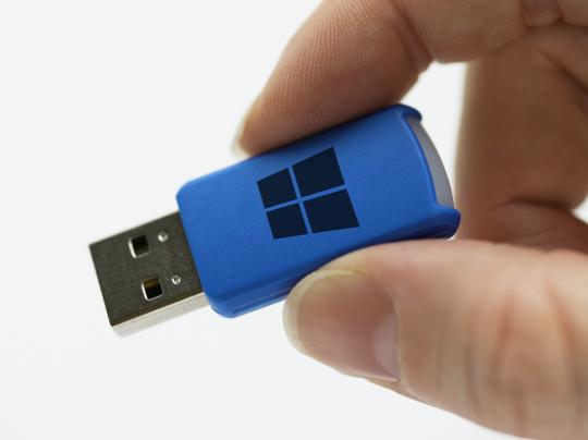
According to information allegedly obtained by German news site WinFuture, some retail versions of Windows 10 will be sold on preloaded USB flash drives.
A
Microsoft spokesperson declined to confirm or deny the news, citing the
company’s policy to not comment on rumors or speculation.
The
much-anticipated multi-platform version of Microsoft’s flagship OS is
built to operate not only on full PCs, but also tablets and ultrabook
laptops, most of which don’t typically pack a CD or DVD drive. A USB
thumb drive version would allow smaller, next-gen machines to also
install Windows 10 Home or Professionial versions from scratch without a
lengthy download.
The full-install version of Windows 10, set to be released on July 29, will start at $119.
Of course, since Microsoft has announced that Windows 10 will come as a free, downloadable update for current Windows 7 and Windows 8 customers, most PCers will never need to see a Windows 10 disc or flash drive.
But hey, by slowly eschewing plastic discs and finally
giving us a version of Windows that’s better than Windows XP, Microsoft
is already well on its way toward embracing 21st century technology.
Way to go, Redmond!
PC-on-a-stick
From Wikipedia, the free encyclopedia
PC-on-a-stick (also known as Stick PC and Compute Stick) is a
term describing PC technology characterized by a small form factor
device that resembles a "dongle", generally using a ARM or Intel Atomsystem on a chip,
low energy usage which offers portable convenience and low prices. It
is actually quite useful because it is a small portable computer.
Existing devices
Lenovo IdeaCenter S 300 - Windows 8.1
iBall Splendo - Windows 8.1
Asus Pen Stick - Windows 10
Google Chromecast - Marvell DE3005 powered and function limited computer with Google services pre-installed.
Intel Compute Stick
STCK1A32WFC - Windows 8.1 (with Bing) pc-on-a-stick powered by Intel
Atom Z3735F Quad Core CPU. 2GB DDR3 RAM (soldered) and 32GB eMMC ROM
(also soldered). Very similar to the Hannspree Micro PC that was
released four months prior to it except that the Compute Stick features a
mini-fan that actively cools the device and facilitates greater
processing usage.[1]
IGEP COM MODULE - PC-on-a-stick version of IGEPv2 from ISEE
RikomagicMK802 and MK802 II - China-made computer in PC-on-a-stick format using AllWinner A1X
Cortex-A8 processor at 1.5 GHz with a Mali 400MP GPU and 512 MB (1 GB
for vII) of DDR3 RAM, Android 4.0 The MK802 III use instead a Rockchip
RK3066.
MK808 - China-made computer in PC-on-a-stick format using Rockchip RK3066 dual-core 1.6 GHz ARM Cortex-A9 MPCore processor with a quad-core Mali-400M GPU and 1 GB of DDR3 RAM, Android 4.1.1
Kimdecent Androstick using Amlogic 8726 SoC (ARM Cortex-A9 @ 1 GHz, Mali-400MP), with 512 MB of RAM.
Zealz GK802/Haipad HI802 - Android stick PC using a Freescale i.MX6Q
quad-core ARM Cortex-A9 processor with Vivante GC2000 GPU and 1 GB DDR3
RAM. Can also run Ubuntu as well as Android.[2]
Hannspree Micro PC - Windows 8.1 based HDMI stick PC running on an
Intel Atom Z3735F 1.33 GHz processor, 2 GB DDR3 RAM, 32 GB eMMC with
802.11bgn/Bluetooth 4.0 [3]
Roku Streaming Stick - HDMI dongle using 512 MB RAM, 256 MB of storage (ROM),[4] 802.11 dual-band (a/b/g/n compatible) [5] that outputs both 720p and 1080p video.
Amazon Fire TV Stick - Dual-core Broadcom Capri 28155 (2xARM
Cortex-A9 up to 1 GHz) HDMI stick with 1 GB RAM, 8 GB ROM,
dual-band/dual-antenna Wi-Fi (802.11a/b/g/n).[6]
Beelink Pocket P2 - Another Intel Atom (Z3735F) quad-core based stick PC with 2 GB RAM and 32 GB ROM that runs Windows 8.1.
CloudPlug, a plug computer developed by CTERA Networks
Seagate Dockstar, a plug computer similar to the SheevaPlug
A plug computer is an external device, often configured for use in the home
or office as a compact computer. It consists of a high-performance,
low-power system-on-a-chip processor with several I/O ports (USB ports,
...) and typically runs any of a number of [Linux] distributions. Most
versions do not have provisions for connecting a display and are best
suited as for running media server, back-up services, file sharing and remote access functions, thus acting as a bridge between in-home protocols such as Digital Living Network Alliance (DLNA) and Server Message Block (SMB) and cloud based services. There are, however, plug computer offerings that have analog VGA monitor and/or HDMI
connectors, which, along with multiple USB ports, permit the use of a
display, keyboard, and mouse, thus making them full-fledged, low-power
alternatives to desktop and notebook computers.
The name "plug computer" is derived from the small configuration of such devices: plug computers are often enclosed in an AC power plug or AC adapter.
Plug computers typically consume little power and are inexpensive. One manufacturer claims its $119 plug computer draws 1.2 watts and can cost $2 a year to run.[1]
On January 6, 2009 CTERA Networks launched a device called CloudPlug that provides online backup at local disk speeds and overlays a file sharing service.[2] The device also transforms any external USB hard drive into a network-attached storage device.[3][4]
On January 7, 2009, Cloud Engines unveiled Pogoplug network access server.[5][6][7][8]
On January 8, 2009, Axentra announced availability of their HipServ platform.[9]
On August 19, 2009, CodeLathe announced availability of their TonidoPlug network access server.[12]
On November 13, 2009 QuadAxis launched its plug computing device product line and development platform, featuring the QuadPlug and QuadPC and running QuadMix, a modified Linux.[13]
On January 5, 2010, Iomega announced their iConnect network access server.[14]
On January 7, 2010 Pbxnsip launched its plug computing device the sipJack running pbxnsip: an IP Communications platform.[15]
One of the first 10 MMD-1s, a prototype unit, produced by E&L
Instruments in 1976. The "dyna-micro"/"MMD-1" was the world's first true
single board computer. The MMD-1 had all components on a single printed circuit board,
including memory, I/O, user input device, and a display. Nothing
external to the single board except power was required to both program
and run the MMD-1. The original design of the MMD-1 was called the
"dyna-micro", but it was soon re-branded as the "MMD-1"
A socket 3 based 486 SBC with power supply and flatscreen
Close up of SBC
A single-board computer (SBC) is a complete computer built on a single circuit board, with microprocessor(s), memory, input/output
(I/O) and other features required of a functional computer.
Single-board computers were made as demonstration or development
systems, for educational systems, or for use as embedded computer controllers. Many types of home computer or portable computer integrated all their functions onto a single printed circuit board.
Unlike a desktop personal computer,
single board computers often did not rely on expansion slots for
peripheral functions or expansion. Some single-board computers are made
to plug into a backplane
for system expansion. Single board computers have been built using a
wide range of microprocessors. Simple designs, such as built by computer
hobbyists, often use static RAM and low-cost 8 or 16 bit processors. Other types, such as blade servers, include all the memory and processor performance of a server computer in a compact space-saving format.
The first true single-board computer (see the May 1976 issue of Radio-Electronics) called the "dyna-micro" was based on the Intel C8080A, and also used Intel's first EPROM, the C1702A. The dyna-micro was re-branded by E&L Instruments of Derby, CT in 1976 as the "MMD-1" (Mini-Micro Designer 1) and was made famous as the example microcomputer in the very popular 8080 "BugBook" series of the time. SBCs also figured heavily in the early history of home computers, for example in the Acorn Electron and the BBC Micro. Other typical early single board computers like the KIM-1 were often shipped without enclosure, which had to be added by the owner, other examples are the Ferguson Big Board and the Nascom. With the development of PCs there was a sharp shift away from SBC, with computers being constructed from a motherboard,
with functions like serial ports, disk drive controller and graphics
being provided on daughterboards. The recent availability of advanced
chip sets providing most of the I/O features as embedded components
allows motherboard manufacturers to offer motherboards with I/O
traditionally provided by daughterboards. Most PC motherboards now offer
on-board support for disk drives including IDE and SATA with RAID, graphics, Ethernet,
and traditional I/O such as serial and parallel ports, USB, and
keyboard/mouse support. Plug-in cards are now more commonly high
performance graphics cards (really graphics co-processors), high end
RAID controllers, and specialized I/O cards such as data acquisition and
DSP (Digital Signal Processor) boards.
Applications
Single board computers were made possible by increasing density of integrated circuits.
A single-board configuration reduces a system's overall cost, by
reducing the number of circuit boards required, and by eliminating
connectors and bus driver circuits that would otherwise be used. By
putting all the functions on one board, a smaller overall system can be
obtained, for example, as in notebook computers. Connectors are a
frequent source of reliability problems, so a single-board system
eliminates these problems. [1]
Single board computers are now commonly defined across two distinct architectures: no slots and slot support. Embedded
SBCs are units providing all the required I/O with no provision for
plug-in cards. Applications are typically gaming (slot machines, video
poker), kiosk, and machine control. Embedded SBCs are much smaller than
the ATX-type motherboard
found in PCs, and provide an I/O mix more targeted to an industrial
application, such as on-board digital and analog I/O, on-board bootable
flash memory (eliminating the need for a disk drive), no video, etc.
The term "Single Board Computer" now generally applies to an architecture where the single board computer is plugged into a backplane to provide for I/O cards. In the case of PC104, the bus is not a backplane in the traditional sense but is a series of pin connectors allowing I/O boards to be stacked.
Single board computers are most commonly used in industrial situations where they are used in rackmount format for process control or embedded
within other devices to provide control and interfacing. Because of the
very high levels of integration, reduced component counts and reduced
connector counts, SBCs are often smaller, lighter, more power efficient
and more reliable than comparable multi-board computers.
The primary advantage of an ATX motherboard as compared to an SBC is
cost. Motherboards are manufactured by the millions for the consumer and
office markets allowing tremendous economies of scale. Single Board
Computers, on the other hand, are in a specialized market niche and are
manufactured in much smaller numbers with the resultant higher cost.
Motherboards and SBCs now offer similar levels of feature integration
meaning that a motherboard failure in either standard will require
equivalent replacement.
The primary advantage of a PICMG Single Board Computer is the
availability of backplanes offering virtually any slot configuration
including legacy ISA support. Motherboards tend to the latest slot
technology such that PCI slots are becoming legacy support with PCI Express
becoming the standard. In addition, motherboards offer, at most, 7
slots while backplanes can offer up to 20 slots. In a backplane 12.3"
wide, similar in size to an ATX motherboard at 12", a backplane with a
Single Board Computer can offer 12 slots for I/O cards with virtually
any mix of slot types.[2]
Types, standards
Major components on an PICMG 1.3 SBC
PICMG 1.3 single-board computer (SHB) and backplane
One common variety of single board computer uses standardized form factors intended for use in a backplane enclosure. Some of these types are CompactPCI, PXI, VMEbus, VXI, and PICMG.
SBCs have been built around various internal processing structures
including the Intel architecture, multiprocessing architectures, and
lower power processing systems like RISC and SPARC. In the Intel PC
world, the intelligence and interface/control circuitry is placed on a
plug-in board that is then inserted into a passive (or active)
backplane. The end result is similar to having a system built with a motherboard,
except that the backplane determines the slot configuration. Backplanes
are available with a mix of slots (ISA, PCI, PCIX, PCI-Express, etc.),
usually totaling 20 or fewer, meaning it will fit in a 19" rackmount
enclosure (17" wide chassis).
Some single-board computers have connectors which allow a stack of
circuit boards, each containing expansion hardware, to be assembled
without a traditional backplane. Examples of stacking SBC form factors
include PC/104, PC/104-Plus, PCI-104, EPIC, and EBX; these systems are commonly available for use in embedded control systems. PICMG provides standards for the backplane interface: PICMG 1.0, 1.1 and 1.2[3] provide for ISA and PCI support with 1.2 adding PCIX support. PICMG 1.3[4][5] provides for PCI-Express support. single-board computers meeting the PICMG 1.3 specification are referred to as a System Host Board (SHB).
Stack-type SBCs often have memory provided on plug-cards such as SIMMs and DIMMs. Hard drive
circuit boards are also not counted for determining if a computer is an
SBC or not for two reasons, firstly because the HDD is regarded as a
single block storage unit, and secondly because the SBC may not require a
hard drive at all as most can be booted from their network connections.
The following is a list of open-source hardware projects that includes computer systems and components.
Bug Labs – a handheld prototyping system based on the Texas Instruments OMAP3530 with ARM Cortex-A8 (600 MHz) and Angstrom Linux.
Ethernut – open-source electronics prototyping platform for building tiny embedded Ethernet devices.
Milkymist One – Single-board computer implementing all the core logic with open source Verilog HDL design files, which is confidential and proprietary in most other open-source hardware computers. It is an interactive VJ station featuring the open-source Milkymist SoC as CPU.
PLAICE
– The PLAICE is an open-source hardware and software project developing
a powerful in-circuit development tool that combines in one device the
features of a FLASH Programmer, Memory Emulator, and High Speed
Multi-Channel Logic Analyzer. It runs uClinux.
Simputer – handheld computer aimed at developing countries
Tinkerforge - Bricks and Bricklets (Modular hardware kit).
Project Turris - open hardware and software WiFi and Ethernet
routers, ready for hacking and tinkering. It runs an OpenWRT based OS [4]
Boards
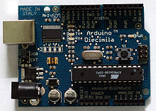
Arduino, an open-source physical computing platform based on a simple I/O board and a development environment that implements the open source Processing / Wiring language. Also clones of this platform including Freeduino.
LEON is an open source 32-bit SPARC-like CPU created by the ESA. It's the standard CPU for the European Space Industry.
Milkymist SoC, featuring the LatticeMico32 microprocessor core, has a complete set of independently developed open source system-on-chip cores such as a SDRAM controller, bus components, graphics accelerators and a variety of I/O devices.
OpenCores
is a loose community of designers that supports open-source cores
(logic designs) for CPUs, peripherals and other devices. OpenCores
maintains an open-source on-chip interconnection bus specification
called Wishbone.
Nyuzi Processor - an GPL/LGPL-licensed GPGPU processor design. Nyuzi Processor is fully open-source with its Verilog, documentation, tests, compiler and tools.[6]
A single-board microcontroller is a microcontroller built onto a single printed circuit board. This board provides all of the circuitry necessary for a useful control task: microprocessor, I/O circuits, clock generator, RAM, stored program memory and any support ICs
necessary. The intention is that the board is immediately useful to an
application developer, without them needing to spend time and effort in
developing the controller hardware.
As they are usually low-cost hardware, and have an especially low
capital cost for development, single-board microcontrollers have long
been popular in education. They are also a popular means for developers
to gain hands-on experience with a new processor family.
Single-board microcontrollers appeared in the late 1970s when the first generations of microprocessors, such as the 6502 and the Z80,[1]
made it practical to build an entire controller on a single board, and
affordable to dedicate a computer to a relatively minor task.
In March 1976, Intel announced a single-board computer product that integrated all the support components required for their 8080
microprocessor, along with 1 kbyte of RAM, 4 kbytes of
user-programmable ROM, and 48 lines of parallel digital I/O with line
drivers. The board also offered expansion through a bus connector, but
it could be used without an expansion card cage where applications
didn't require additional hardware. Software development for this system
was hosted on Intel's Intellec MDS microcomputer development system; this provided assembler and PL/M support, and permitted in-circuit emulation for debugging.[2]
Processors of this era required a number of support chips in addition. RAM and EPROM were separate, often requiring memory management or refresh circuitry for dynamic memory as well. I/O processing might be carried out by a single chip such as the 8255, but frequently required several more chips.
A single-board microcontroller differs from a single-board computer
in that it lacks the general purpose user interface and mass storage
interfaces that a more general-purpose computer would have. Compared to a
microprocessor development board,
a microcontroller board would emphasize digital and analog control
interconnections to some controlled system, where a development board
might by comparison have only a few or no discrete or analog
input/output devices. The development board exists to showcase or to
train on some particular processor family and this internal
implementation is more important than the external function.
Internal bus
The bus of the early single-board devices, such as the Z80 and 6502, was universally a Von Neumann architecture.
Program and data memory were accessed by the same shared bus, even
though they were stored in fundamentally different types of memory: ROM for programs and RAM
for data. This bus architecture was needed to economise on the number
of pins needed from the limited 40 available for the processor's
ubiquitous dual-in-line IC package.
It was common to offer the internal bus through an expansion
connector, or at least the space for such a connector to be soldered on.
This was a low-cost option and offered the potential for expansion,
even if it was rarely made use of. Typical expansions would be I/O
devices, or memory expansion. It was unusual to add peripheral devices
such as tape or disk storage, or even a CRT display
When single-chip microcontrollers, such as the 8048,
became available later on, the bus no longer needed to be exposed
outside the package as all the necessary memory could be provided within
the chip package. This generation of processors used a Harvard architecture of separate program and data buses, both internal to the chip. Many of these processors used a modified Harvard architecture,
where some write access was possible to the program data space, thus
permitting in-circuit programming. None of these processors required, or
supported, a Harvard bus across a single-board microcontroller. Where
they supported a bus for expansion of peripherals, this used a dedicated
I/O bus, such as I2C, One-wire or various serial buses.
External bus expansion
Some microcontroller boards using a general-purpose microprocessor
can bring the address and data bus of the processor to an expansion
connector, allowing additional memory or peripherals to be added. This
would provide resources not already present on the single board system.
Since not all systems require expansion, the connector may be an option,
with a mounting position provided for the connector for installation by
the user if desired.
Microcontroller systems provide multiple forms of input and output
signals to allow application software to control an external
"real-world" system. Discrete digital I/O provides a single bit of data
(on, or off). Analog signals, representing a continuously variable range
such as temperature or pressure, can also be inputs and outputs for
microcontrollers.
Discrete digital inputs and outputs might only be buffered from the
microprocessor data bus by an addressable latch, or might be operated by
a specialized input/output integrated circuit such as an Intel 8255 or Motorola 6821 parallel input/output adapter.
Later single-chip micrcontrollers have input and output pins available.
The input/output circuits usually do not provide enough current to
directly operate such devices as lamps or motors, so solid-state relays
are operated by the microcontroller digital outputs, and inputs are
isolated by signal conditioning level-shifting and protection circuits.
One or more analog inputs, with an analog multiplexer and common
analog to digital converter, are found on some microcontroller boards.
Analog outputs may use a digital-to-analog converter, or on some
microcontrollers may be controlled by pulse-width modulation. As for discrete inputs, external circuits may be required to scale inputs, or to provide such functions as bridge excitation or cold junction compensation.
To control component costs, many boards were designed with extra
hardware interface circuits but the components for these circuits
weren't installed and the board was left bare. The circuit was only
added as an option on delivery, or could be populated later.
It is common practice for boards to include "prototyping areas",
areas of the board already laid out as a solderable breadboard area with
the bus and power rails available, but without a defined circuit.
Several controllers, particularly those intended for training, also
include a pluggable re-usable breadboard for easy prototyping of extra I/O circuits that could be changed or removed for later projects.
Communications and user interfaces
Communications interfaces vary depending on the age of the microcontroller system. Early systems might implement a serial port to provide RS-232 or current loop.
The serial port could be used by the application program, or could be
used, in conjunction with a monitor ROM, to transfer programs into the
microcontroller memory. Current microcontrollers may support USB, wireless network (Wi-Fi, ZigBee, or others) ports, or provide an Ethernet connection, and may support a TCP/IP
protocol stack. Some devices have firmware available to implement a Web
server, allowing an application developer to rapidly build a
Web-enabled instrument or system.
Programming
Many of the earliest systems had no internal facility for programming
at all, and relied on a separate "host" system. This programming was
typically in assembly language, sometimes C or even PL/M, and then cross-assembled or cross-compiled
on the host. Some single-board microcontrollers support a BASIC
language system, allowing programs to be developed on the target
hardware. Hosted development allows all the storage and peripherals of a
desktop computer to be used, providing a more powerful development
environment.
EPROM burning
Early microcontrollers relied on erasable programmable read-only memory (EPROM) devices to hold the application program. The completed object code from a host system would be "burned" onto an EPROM with an EPROM programmer,[3]
this EPROM was then physically plugged into the board. As the EPROM
would be removed and replaced many times during program development, it
was usual to provide a ZIF socket to avoid wear or damage. Erasing an EPROM with a UV
eraser takes a considerable time, and so it was also usual for a
developer to have several EPROMs in circulation at any one time.
Some microcontroller devices were available with on-board EPROM;
these, too, would be programmed in a separate burner, then put into a
socket on the target system.
The use of EPROM sockets allowed field update of the application program, either to fix errors or to provide updated features.
Keypad monitors
A single-board computer with a hex keypad and 7-segment display
Where the single-board controller formed the entire development
environment (typically in education) the board might also be provided
with a simple hexadecimal keypad, calculator-style LED display and a "monitor" program set permanently in ROM. This monitor allowed machine code
programs to be entered directly through the keyboard and held in RAM.
These programs were in machine code, not even in assembly language, and
were assembled by hand on paper first. It's arguable as to which process
was more time-consuming and error prone: assembling by hand, or keying
byte-by-byte.
Single-board "keypad and calculator display" microcontrollers of this
type were very similar to some low-end microcomputers of the time, such
as the KIM-1 or the Microprofessor I.[4]
Some of these microprocessor "trainer" systems are still in production
today, as a very low-cost introduction to microprocessors at the
hardware programming level.[5]
Hosted development
When desktop personal computers appeared, initially CP/M or Apple II, then later the IBM PC
and compatibles, there was a shift to hosted development. Hardware was
now cheaper and RAM capacity had expanded such that it was possible to
download the program through the serial port and hold it in RAM. This
massive reduction in the cycle time to test a new version of a program
gave an equally large boost in development speed.
This program memory was still volatile and would be lost if power was turned off. Flash memory
was not yet available at a viable price. As a completed controller
project usually required to be non-volatile, the final step in a project
was often to burn an EPROM again.
Single-chip microcontrollers
A 8048-family microcontroller with on-board UV EPROM, the 8749
Single-chip microcontrollers such as the 8748
combined many of the features of the previous boards into a single IC
package. Single-chip microcontrollers integrate memory (both RAM and
ROM) on-package and so do not need to expose the data and address bus
through the IC package's pins. These pins are then available for I/O
lines. These changes reduce the area required on a printed circuit board
and simplify the design of a single-board microcontroller. Examples of
single-chip microcontrollers include:
For production use as embedded systems, the on-board ROM would be either mask programmed at the chip factory or one-time programmed (OTP) by the developer as a PROM.
PROMs often used the same UV EPROM technology for the chip, but in a
cheaper package without the transparent erasure window. During program
development it was still necessary to burn EPROMs, this time the entire
controller IC, and so ZIF sockets would be provided.
With the development of affordable EEPROM and eventually flash memory,
it became practical to attach the controller permanently to the board
and to download program code to it through a serial connection to a host
computer. This was termed "in-circuit programming".
Erasure of old programs was carried out by either over-writing them
with a new download, or bulk erasing them electrically (for EEPROM) which was slower, but could be carried out in-situ.
The main function of the controller board was now to carry the support circuits for this serial interface, or USB
on later boards. As a further convenience feature during development,
many boards also carried low-cost features like LED monitors of the I/O
lines or reset switches mounted on board.
Microcontrollers are now cheap and simple to design circuit boards
for. Development host systems are also cheap, especially when using open source software. Higher level programming languages abstract
details of the hardware, making differences between specific processors
less obvious to the application programmer. Rewritable flash memory has
replaced slow programming cycles, at least during program development.
Accordingly almost all development now is based on cross-compilation
from personal computers and download to the controller board through a
serial-like interface, usually appearing to the host as a USB device.
The original market demand of a simplified board implementation is no
longer so relevant to microcontrollers. Single-board microcontrollers
are still important, but have shifted their focus to:
Easily accessible platforms aimed at traditionally "non-programmer"
groups, such as artists, designers, hobbyists, and others interested in
creating interactive objects or environments.[6]
Some typical projects in 2011 included; the backup control of DMX stage
lights and special effects, multi-camera control, autonomous fighting
robots, controlling bluetooth projects from a computer or smart phone,[7] LEDs and multiplexing, displays, audio, motors, mechanics, and power control.[8] These controllers may be embedded to form part of a physical computing project. Popular choices for this work are the Arduino,[9]Dwengo[7] or the Wiring (development platform).[10][11]
Technology demonstrator boards for innovative processors or peripheral features:
Adapteva is a fablesssemiconductor company focusing on low power multi-core
microprocessor design. The company was the second company to announce a
design with 1,000 specialized processing cores on a single chip.[1][2]
The company name is a combination of "adapt" and the Hebrew word
"Teva" meaning nature. The name is a reflection of the company's key
technology and business philosophy.
Adapteva was founded in March 2008 by Andreas Olofsson. The company
was founded with the goal of bringing a 10× advancement in floating
point processing energy efficiency for the mobile device market. In May
2009, Mr. Olofsson had taped out the first prototype based on a new type
of massively parallel
multi-core computer architecture. The initial prototype was implemented
in 65 nm and had 16 independent microprocessor cores. The initial
prototypes enabled Adapteva to secure US$1.5M in Series-A funding from
BittWare, a company from Concord, New Hampshire, in October 2009.[3]
Adapteva's first commercial chip product started sampling to
customers in early May 2011 and they soon thereafter announced the
capability to put up to 4,096 cores on a single chip.
The current version, Epiphany III, was announced in October
2011 and has been taped-out at 28 nm and is available in 65nm, while the
64-cores, 28nm version was said to be generally available in January
2012, and has been sampled and shipped but isn't generally available as
of August 2014.
Products
Adapteva's main product family is the Epiphany scalable multi-core MIMD architecture. The Epiphany architecture could accommodate chips with up to 4,096 RISCout-of-ordermicroprocessors, all sharing a single 32-bit flat memory space. Each RISC processor in the Epiphany architecture is superscalar with 64× 32-bit unified register file (integer or single precision) microprocessor operating up to 1 GHz and capable of 2 GFLOPS (single precision). Epiphany's RISC processors use a custom instruction set architecture (ISA) optimised for single precision floating point,[4] but are programmable in high level ANSI C using a standard GNU-GCC tool chain. Each RISC processor (in current implementations; not fixed in the architecture) has 32 KB
of local memory. Code (possibly duplicated in each core) and stack
space should be in that local memory; in addition (most) data should fit
there for full speed. Data can also be used from other processor cores
local memory at a speed penalty or off-chip RAM with much larger speed
penalty. The memory architecture is unusual in that it doesn't employ
explicit hierarchy or hardware caches.
The flat and unobstructed memory hierarchy allows cores to communicate
with each other efficiently, reducing overhead in core-to-core
communication. All processor nodes are connected through a Network On Chip.[5]
Epiphany multi-core coprocessors
16-core Adapteva Epiphany chip, E16G301, from Parallella single-board computer.
On August 19, 2012, Adapteva posted some specifications and information about Epiphany multi-core coprocessors.[6]
n September 2012, a 16-core version, the Epiphany-III (E16G301), was produced using 65 nm[9] (11.5 mm2, 500 MHz chip[10]) and engineering samples of 64-core Epiphany-IV (E64G401) were produced using 28 nm GlobalFoundries process (800 MHz).[11]
The primary markets for the Epiphany multi-core architecture include:
Parallella single-board computer with 16-core Epiphany chip and Zynq-7010 FPGA.
In September 2012, Adapteva started project Parallella on Kickstarter, which was marketed as "A Supercomputer for everyone." Architecture reference manuals for the platform were published as part of the campaign to attract attention to the project.[12]
The US$750,000 funding goal was reached in a month, with a minimum
contribution of US$99 entitling backers to obtain one device; although
the initial deadline was set for May 2013, the first single-board
computers with 16-core Epiphany chip were finally shipped in December
2013.[13]
Size of board is planned to be 86 mm × 53 mm (3.4 in × 2.1 in).[14][15][16]
The campaign successfully raised US$898,921 via the Kickstarter campaign.[17][18] Raising US$3 million goal was unsuccessful, so no 64-core version of Parallella will be mass-produced.[19] Kickstarter users having donated more than US$750 will get "parallella-64" variant with 64-core coprocessor (made from initial prototype manufacturing with 50 chips yield per wafer).[20]
Performance
Joel Hruska from Extremetech has the following derogatory opinion
about this project: "Adapteva is drastically overselling what the
Epiphany IV can actually deliver. 16–64 tiny cores with small amounts of
memory, no local caches, and a relatively low clock speed can still be
useful in certain workloads, but contributors aren’t buying a
supercomputer — they’re buying the real-world equivalent of a
self-sealing stem bolt."[22]
The criticism that the Epiphany chips cannot provide anywhere near
the performance of modern supercomputers is nevertheless correct:
actually, current Epiphany chips with 16-cores or 64-cores and c. 25 or
100 GFLOPs in single precision, respectively, do not even match the
floating-point performance of modern desktop PC processors (Core
i7-4770K (Haswell), 4× cores @ 3.5 GHz AVX2: 177 GFLOPS,[23] double precision) – a fact that is acknowledged by Adapteva.
However, the latest Parallella boards with E16 Epiphany chips[24]
can be compared to many ancient supercomputers in terms of raw
performance (just as an example, the Cray 1 – the first supercomputer
per se – had a peak performance of 80 MFLOPS
at 1976, and its successor the Cray 2 had a peak performance of
1.9 GFLOPS at 1985), and can certainly be used for parallel code
development.
The point being that for a power envelope of 5 W and in terms of GFLOPS/mm2 of chip die space, the current E16 Epiphany chips provide vastly more performance than anything else available to date.[citation needed]
The 16-core Parallella has roughly 5.0 GFLOPs/W, and the 64-core
Epiphany-IV made with 28 nm estimated as 50 GFLOPs/W (single precision),[25] and 32-board system based on them has 15 GFLOPS/W.[26] For comparison, top GPUs from AMD and Nvidia reached 10 GFLOPs/W for single precision in 2009–2011 timeframe.[27]
Multi-core processor
From Wikipedia, the free encyclopedia
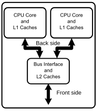
Diagram of a generic dual-core processor with CPU-local level-1 caches and a shared, on-die level-2 cache
A multi-core processor is a single computing component with two or more independent actual processing units (called "cores"), which are the units that read and execute program instructions.[1] The instructions are ordinary CPU instructions
such as add, move data, and branch, but the multiple cores can run
multiple instructions at the same time, increasing overall speed for
programs amenable to parallel computing.[2] Manufacturers typically integrate the cores onto a single integrated circuitdie (known as a chip multiprocessor or CMP), or onto multiple dies in a single chip package.
Processors were originally developed with only one core. In the mid 1980s Rockwell International manufactured versions of the 6502 with two 6502 cores on one chip as the R65C00, R65C21, and R65C29,[3][4] sharing the chip's pins on alternate clock phases. Other multi-core processors were developed in the early 2000s by Intel, AMD and others.
Multi-core processors may have two cores (dual-core CPUs, for example, AMD Phenom II X2 and Intel Core Duo), four cores (quad-core CPUs, for example, AMD Phenom II X4, Intel's i5 and i7 processors), six cores (hexa-core CPUs, for example, AMD Phenom II X6 and Intel Core i7 Extreme Edition 980X), eight cores (octo-core CPUs, for example, Intel Xeon E7-2820 and AMD FX-8350), ten cores (for example, Intel Xeon E7-2850), or more.
A multi-core processor implements multiprocessing
in a single physical package. Designers may couple cores in a
multi-core device tightly or loosely. For example, cores may or may not
share caches, and they may implement message passing or shared-memory inter-core communication methods. Common network topologies to interconnect cores include bus, ring, two-dimensional mesh, and crossbar. Homogeneous multi-core systems include only identical cores, heterogeneous
multi-core systems have cores that are not identical. Just as with
single-processor systems, cores in multi-core systems may implement
architectures such as superscalar, VLIW, vector processing, SIMD, or multithreading.
Multi-core processors are widely used across many application domains including general-purpose, embedded, network, digital signal processing (DSP), and graphics.
The improvement in performance gained by the use of a multi-core
processor depends very much on the software algorithms used and their
implementation. In particular, possible gains are limited by the
fraction of the software that can be run in parallel simultaneously on multiple cores; this effect is described by Amdahl's law. In the best case, so-called embarrassingly parallel
problems may realize speedup factors near the number of cores, or even
more if the problem is split up enough to fit within each core's
cache(s), avoiding use of much slower main system memory. Most
applications, however, are not accelerated so much unless programmers
invest a prohibitive amount of effort in re-factoring the whole problem.[5] The parallelization of software is a significant ongoing topic of research.
The terms multi-core and dual-core most commonly refer to some sort of central processing unit (CPU), but are sometimes also applied to digital signal processors (DSP) and system-on-a-chip (SoC). The terms are generally used only to refer to multi-core microprocessors that are manufactured on the same integrated circuit die; separate microprocessor dies in the same package are generally referred to by another name, such as multi-chip module. This article uses the terms "multi-core" and "dual-core" for CPUs manufactured on the same integrated circuit, unless otherwise noted.
In contrast to multi-core systems, the term multi-CPU refers
to multiple physically separate processing-units (which often contain
special circuitry to facilitate communication between each other).
The terms many-core and massively multi-core are sometimes used to describe multi-core architectures with an especially high number of cores (tens or hundreds).[6]
Some systems use many soft microprocessor cores placed on a single FPGA. Each "core" can be considered a "semiconductor intellectual property core" as well as a CPU core[citation needed].
Development
While manufacturing technology improves, reducing the size of individual gates, physical limits of semiconductor-based microelectronics
have become a major design concern. These physical limitations can
cause significant heat dissipation and data synchronization problems.
Various other methods are used to improve CPU performance. Some instruction-level parallelism (ILP) methods such as superscalarpipelining
are suitable for many applications, but are inefficient for others that
contain difficult-to-predict code. Many applications are better suited
to thread-level parallelism
(TLP) methods, and multiple independent CPUs are commonly used to
increase a system's overall TLP. A combination of increased available
space (due to refined manufacturing processes) and the demand for
increased TLP led to the development of multi-core CPUs.
Commercial incentives
Several business motives drive the development of multi-core
architectures. For decades, it was possible to improve performance of a
CPU by shrinking the area of the integrated circuit (IC), which drove
down the cost per device on the IC. Alternatively, for the same circuit
area, more transistors could be used in the design, which increased
functionality, especially for complex instruction set computing (CISC) architectures. Clock rates
also increased by orders of magnitude in the decades of the late 20th
century, from several megahertz in the 1980s to several gigahertz in the
early 2000s.
As the rate of clock speed improvements slowed, increased use of
parallel computing in the form of multi-core processors has been pursued
to improve overall processing performance. Multiple cores were used on
the same CPU chip, which could then lead to better sales of CPU chips
with two or more cores. Intel has produced a 48-core processor for
research in cloud computing; each core has an x86 architecture.[7][8]
Technical factors
Since computer manufacturers have long implemented symmetric multiprocessing
(SMP) designs using discrete CPUs, the issues regarding implementing
multi-core processor architecture and supporting it with software are
well known.
Additionally:
Using a proven processing-core design without architectural changes reduces design risk significantly.
For general-purpose processors, much of the motivation for
multi-core processors comes from greatly diminished gains in processor
performance from increasing the operating frequency. This is due to three primary factors:
The memory wall; the increasing gap between processor and
memory speeds. This, in effect, pushes for cache sizes to be larger in
order to mask the latency of memory. This helps only to the extent that
memory bandwidth is not the bottleneck in performance.
The power wall; the trend of consuming exponentially
increasing power with each factorial increase of operating frequency.
This increase can be mitigated by "shrinking" the processor by using smaller traces for the same logic. The power wall
poses manufacturing, system design and deployment problems that have
not been justified in the face of the diminished gains in performance
due to the memory wall and ILP wall.
In order to continue delivering regular performance improvements for general-purpose processors, manufacturers such as Intel and AMD
have turned to multi-core designs, sacrificing lower
manufacturing-costs for higher performance in some applications and
systems. Multi-core architectures are being developed, but so are the
alternatives. An especially strong contender for established markets is
the further integration of peripheral functions into the chip.
Advantages
The proximity of multiple CPU cores on the same die allows the cache coherency
circuitry to operate at a much higher clock rate than is possible if
the signals have to travel off-chip. Combining equivalent CPUs on a
single die significantly improves the performance of cache snoop (alternative: Bus snooping) operations. Put simply, this means that signals between different CPUs travel shorter distances, and therefore those signals degrade
less. These higher-quality signals allow more data to be sent in a
given time period, since individual signals can be shorter and do not
need to be repeated as often.
Assuming that the die can physically fit into the package, multi-core CPU designs require much less printed circuit board
(PCB) space than do multi-chip SMP designs. Also, a dual-core processor
uses slightly less power than two coupled single-core processors,
principally because of the decreased power required to drive signals
external to the chip. Furthermore, the cores share some circuitry, like
the L2 cache and the interface to the front-side bus
(FSB). In terms of competing technologies for the available silicon die
area, multi-core design can make use of proven CPU core library designs
and produce a product with lower risk of design error than devising a
new wider-core design. Also, adding more cache suffers from diminishing
returns.[citation needed]
Multi-core chips also allow higher performance at lower energy. This
can be a big factor in mobile devices that operate on batteries. Since
each core in a multi-core CPU is generally more energy-efficient, the
chip becomes more efficient than having a single large monolithic core.
This allows higher performance with less energy. The challenge of
writing parallel code clearly offsets this benefit.[9]
Disadvantages
Maximizing the usage of the computing resources provided by multi-core processors requires adjustments both to the operating system
(OS) support and to existing application software. Also, the ability of
multi-core processors to increase application performance depends on
the use of multiple threads within applications.
Integration of a multi-core chip drives chip production yields down.
They are also more difficult to manage thermally than lower-density
single-core designs. Intel has partially countered this first problem by
creating its quad-core designs by combining two dual-core ones on a
single die with a unified cache, hence any two working dual-core dies
can be used, as opposed to producing four cores on a single die and
requiring all four to work to produce a quad-core CPU. From an
architectural point of view, ultimately, single CPU designs may make
better use of the silicon surface area than multiprocessing cores, so a
development commitment to this architecture may carry the risk of
obsolescence. Finally, raw processing power is not the only constraint
on system performance. Two processing cores sharing the same system bus
and memory bandwidth limits the real-world performance advantage. It has
been claimed[by whom?]
that if a single core is close to being memory-bandwidth limited, then
going to dual-core might give 30% to 70% improvement; if memory
bandwidth is not a problem, then a 90% improvement can be expected;
however, Amdahl's law makes this claim dubious.[10]
It would be possible for an application that used two CPUs to end up
running faster on a dual-core one if communication between the CPUs was
the limiting factor, which would count as more than 100% improvement.
Hardware
Trends
The general trend in processor development has moved from dual-,
tri-, quad-, hex-, oct-core chips to ones with tens or even thousands of
cores.[citation needed] In addition, multi-core chips mixed with simultaneous multithreading, memory-on-chip, and special-purpose "heterogeneous"
cores promise further performance and efficiency gains, especially in
processing multimedia, recognition and networking applications. There is
also a trend of improving energy-efficiency by focusing on
performance-per-watt with advanced fine-grain or ultra fine-grain power management and dynamic voltage and frequency scaling (i.e. laptop computers and portable media players).
Architecture
The composition and balance of the cores in multi-core architecture
show great variety. Some architectures use one core design repeated
consistently ("homogeneous"), while others use a mixture of different
cores, each optimized for a different, "heterogeneous" role.
The article "CPU designers debate multi-core future" by Rick Merritt, EE Times 2008,[11] includes these comments:
Chuck Moore [...] suggested computers should be more like cellphones,
using a variety of specialty cores to run modular software scheduled by
a high-level applications programming interface.
[...] Atsushi Hasegawa, a senior chief engineer at Renesas,
generally agreed. He suggested the cellphone's use of many specialty
cores working in concert is a good model for future multi-core designs.
[...] Anant Agarwal, founder and chief executive of startup Tilera,
took the opposing view. He said multi-core chips need to be homogeneous
collections of general-purpose cores to keep the software model simple.
Software effects
An outdated version of an anti-virus application may create a new thread for a scan process, while its GUI
thread waits for commands from the user (e.g. cancel the scan). In such
cases, a multi-core architecture is of little benefit for the
application itself due to the single thread doing all the heavy lifting
and the inability to balance the work evenly across multiple cores.
Programming truly multithreaded code often requires complex
co-ordination of threads and can easily introduce subtle and
difficult-to-find bugs due to the interweaving of processing on data
shared between threads (thread-safety).
Consequently, such code is much more difficult to debug than
single-threaded code when it breaks. There has been a perceived lack of
motivation for writing consumer-level threaded applications because of
the relative rarity of consumer-level demand for maximum use of computer
hardware. Although threaded applications incur little additional
performance penalty on single-processor machines, the extra overhead of
development has been difficult to justify due to the preponderance of
single-processor machines. Also, serial tasks like decoding the entropy encoding algorithms used in video codecs
are impossible to parallelize because each result generated is used to
help create the next result of the entropy decoding algorithm.
Given the increasing emphasis on multi-core chip design, stemming
from the grave thermal and power consumption problems posed by any
further significant increase in processor clock speeds, the extent to
which software can be multithreaded to take advantage of these new chips
is likely to be the single greatest constraint on computer performance
in the future. If developers are unable to design software to fully
exploit the resources provided by multiple cores, then they will
ultimately reach an insurmountable performance ceiling.
The telecommunications market had been one of the first that needed a
new design of parallel datapath packet processing because there was a
very quick adoption of these multiple-core processors for the datapath
and the control plane. These MPUs are going to replace[12] the traditional Network Processors that were based on proprietary micro- or pico-code. Parallel programming techniques can benefit from multiple cores directly. Some existing parallel programming models such as Cilk Plus, OpenMP, OpenHMPP, FastFlow, Skandium, MPI, and Erlang can be used on multi-core platforms. Intel introduced a new abstraction for C++ parallelism called TBB. Other research efforts include the Codeplay Sieve System, Cray's Chapel, Sun's Fortress, and IBM's X10.
Multi-core processing has also affected the ability of modern
computational software development. Developers programming in newer
languages might find that their modern languages do not support
multi-core functionality. This then requires the use of numerical libraries to access code written in languages like C and Fortran, which perform math computations faster than newer languages like C#. Intel's MKL and AMD's ACML
are written in these native languages and take advantage of multi-core
processing. Balancing the application workload across processors can be
problematic, especially if they have different performance
characteristics. There are different conceptual models to deal with the
problem, for example using a coordination language and program building
blocks (programming libraries or higher-order functions). Each block can
have a different native implementation for each processor type. Users
simply program using these abstractions and an intelligent compiler
chooses the best implementation based on the context.[13]
Managing concurrency acquires a central role in developing parallel applications. The basic steps in designing parallel applications are:
Partitioning
The partitioning stage of a design is intended to expose
opportunities for parallel execution. Hence, the focus is on defining a
large number of small tasks in order to yield what is termed a
fine-grained decomposition of a problem.
Communication
The tasks generated by a partition are intended to execute
concurrently but cannot, in general, execute independently. The
computation to be performed in one task will typically require data
associated with another task. Data must then be transferred between
tasks so as to allow computation to proceed. This information flow is
specified in the communication phase of a design.
Agglomeration
In the third stage, development moves from the abstract toward the
concrete. Developers revisit decisions made in the partitioning and
communication phases with a view to obtaining an algorithm that will
execute efficiently on some class of parallel computer. In particular,
developers consider whether it is useful to combine, or agglomerate,
tasks identified by the partitioning phase, so as to provide a smaller
number of tasks, each of greater size. They also determine whether it is
worthwhile to replicate data and computation.
Mapping
In the fourth and final stage of the design of parallel algorithms,
the developers specify where each task is to execute. This mapping
problem does not arise on uniprocessors or on shared-memory computers
that provide automatic task scheduling.
On the other hand, on the server side, multi-core processors are ideal because they allow many users to connect to a site simultaneously and have independent threads of execution. This allows for Web servers and application servers that have much better throughput.
Licensing
Vendors may license some software "per processor". This can give rise
to ambiguity, because a "processor" may consist either of a single core
or of a combination of cores.
Oracle Corporation counts an AMD X2 or an Intel dual-core CPU as a single processor[citation needed] but uses other metrics for other types, especially for processors with more than two cores.[16]
Embedded applications
Embedded computing
operates in an area of processor technology distinct from that of
"mainstream" PCs. The same technological drives towards multi-core apply
here too. Indeed, in many cases the application is a "natural" fit for
multi-core technologies, if the task can easily be partitioned between
the different processors.
In addition, embedded software is typically developed for a specific hardware release, making issues of software portability,
legacy code or supporting independent developers less critical than is
the case for PC or enterprise computing. As a result, it is easier for
developers to adopt new technologies and as a result there is a greater
variety of multi-core processing architectures and suppliers.
As of 2010, multi-core network processing devices have become mainstream, with companies such as Freescale Semiconductor, Cavium Networks, Wintegra and Broadcom
all manufacturing products with eight processors. For the system
developer, a key challenge is how to exploit all the cores in these
devices to achieve maximum networking performance at the system level,
despite the performance limitations inherent in an SMP operating system.
To address this issue, companies such as 6WIND
provide portable packet processing software designed so that the
networking data plane runs in a fast path environment outside the OS,
while retaining full compatibility with standard OS APIs.[17]
In digital signal processing the same trend applies: Texas Instruments has the three-core TMS320C6488 and four-core TMS320C5441, Freescale
the four-core MSC8144 and six-core MSC8156 (and both have stated they
are working on eight-core successors). Newer entries include the Storm-1
family from Stream Processors, Inc with 40 and 80 general purpose ALUs per chip, all programmable in C as a SIMD engine and Picochip with three-hundred processors on a single die, focused on communication applications.
Hardware examples
Commercial
Adapteva
Epiphany, a many-core processor architecture which allows up to 4096
processors on-chip, although only a 16 core version has been
commercially produced.
ARMMPCore is a fully synthesizable multi-core container for ARM11 MPCore and ARM Cortex-A9 MPCore processor cores, intended for high-performance embedded and entertainment applications.
ASOCS ModemX, up to 128 cores, wireless applications.
Sony/IBM/Toshiba's Cell
processor, a nine-core processor with one general purpose PowerPC core
and eight specialized SPUs (Synergystic Processing Unit) optimized for
vector operations used in the SonyPlayStation 3
The research and development of multicore processors often compares
many options, and benchmarks are developed to help such evaluations.
Existing benchmarks include SPLASH-2, PARSEC, and COSMIC for
heterogeneous systems.[21]


No comments:
Post a Comment